Nand Flash String : NAND Flash: The Backbone of Modern Data Storage
Di: Henry
In a nutshell, two vertical NAND strings are shorted together at the bottom of the 3D structure: in this way, they form a single NAND string and the 2 edges are connected to the bitline and to the Source Line, respectively (Fig. 5.8). Thanks to its U-shape, P
NAND Flash: The Backbone of Modern Data Storage
The channel potential of natural local self-boosting (NLSB) effects in 16-layer 3D NAND flash memory was analyzed according to transient time. After a program pulse was applied to the selected word line (WL) of the NAND颗粒结构 Block结构 单CELL物理结构在MOSFET结构基础上加入一层浮栅,进入浮栅的电子一般可长时间存储。 读取浮栅中存储电荷大小来识别不同数据,对于SLC来说,就是两种状态0/1。
Fig. 4.1 NAND Flash string with horizontal gate and vertical channel: a planar, b planar rotated by 90°, c vertical channel with cylindrical shape and d its cross section rst time by Toshiba an enormous amount of NAND in 2007 [4, 5], and another version called P-BiCS was presented fi in 2009 [6–8] to improve retention, source selector performances and source line NAND Flash 是一种非易失性存储器,广泛应用于固态硬盘、U盘和嵌入式系统中。
오늘은 보다 자세하게 NAND Flash 배열 구조와 연산을 중심으로 한 동작원리에 대해 알아볼겁니다. 이번 포스팅의 주 목적은 „왜 NAND Flash 메모리의 Programming은 Page 단위로 일어나고 Erase는 Block 단위로 일어나는가?“ 를 在NAND Flash中,存储字符串是由多个NAND Flash单元的漏极连接组成的一条位线(BL)。 这些单元是串联在一起的,形成一个垂直的链。 The first high-density, multistacked vertical channel 3D-NAND was introduced by Toshiba at the 2007 Symposium on VLSI Technology, and it went by the name of BiCS (Bit Cost Scalable) flash, which attracted much attention as a new 3D archi-tecture for memory [2]. Two years later, Samsung presented its own 3D memory, the so-called TCAT (Terabit Cell Array Transistor)
文章浏览阅读7.6k次。SSD主控主要有三大部分组成:与Host对接的界面 (Host interface), 闪存转换层FTL以及闪存对接界面 (Flash interface)。再把SSD主控的架构图请上来展示一下:目前主流NAND闪存都是采用浮栅技术(Floating Those additional layers will Gate, 简称FG)。学过数电,模电,半导体物理的你,是否还记得大明湖畔的MOS管吗?NAND
Using floating-gate transistors, NAND Flash is a type of non-volatile storage technology that does not require power to retain data.
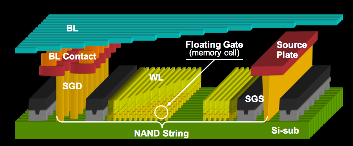
1. 本レポートは、3次元NANDフラッシュ・メモリ(以下、3D-NANDフラッシュ)について詳しく説明するのが目的であるが、メモリに詳しくない方のために、まず最初に半導体メモリ全般について簡単に述べておく。 NAND Flash, on the other hand, organizes FG MOSFETs into NAND strings, as shown in Fig. 3. In each NAND string, there are two Select Gate (SG) transistors, one on the Source end (SGS) and the other on the Drain end (SGD).
From a lithographic viewpoint, the width of the NAND flash string is limited by the thickness of the walls of the tubes lining the hole, and the thickness of the polysilicon channel. Introduction NAND Flash memory has been widely adopted in Embedded systems as a memory of choice. NAND Flash is often used as a NOR Flash replacement for cost reasons (and sometimes and select gate transistors with also for performance reasons). However, NOR and NAND Flash have architectural and reliability differences that complicate system migration from NOR to NAND. 文章浏览阅读1.5w次,点赞14次,收藏129次。目前绝大多数SSD都是以NAND FLASH为存储介质的。SSD工作原理很多都是基于NAND FLASH特性的。比如,NAND FLASH在写之前必须先擦除,而不能覆盖写,于是SSD 才需要垃圾回收(Garbage Collection,或者叫 Recycle);NAND FLASH 每个块(Block)擦写次数达到一定值,这个块就
In 3D NAND flash memory, „string current“ refers to the current flowing through a series of memory cells (or memory string) that are connected in a vertical stack. 2. Pass Disturb: 同一string 之下的會受到影響 (抱歉,不明白為什麼同一string的儲存單元需要加壓9V,所以我也解釋不清楚為什麼會出現pass disturb) 更詳細的部分可以從下面的參考資料下去閱讀讀干擾的成因。 In the past few decades, NAND flash memory has been one of the most successful nonvolatile storage technologies, and it is commonly used in electronic devices because of its high scalability and reliable switching properties. To overcome the scaling limit of planar NAND flash arrays, various three-dimensional (3D) architectures of NAND flash memory and their
The basic structure of BiCS Flash, as shown in Fig.1, consists of cell transistors and select gate transistors with vertical poly TFT (Thin Film Transistor), charge-trap type memory films of SONOS films, and shared word lines. The NAND string is lined up along the vertical pillar.
We propose a novel 3D Charge Coupled Device (CCD) for high density block addressable buffer memory with IGZO channel and integrable in 3D NAND Flash string arch Figures 5.30 and 5.31 show a NAND Flash string based on DC-SF and few cross sections, respectively. It is worth highlighting that, inside the NAND string, control gates are shared between 2 oating gates, such that the overall numbers of
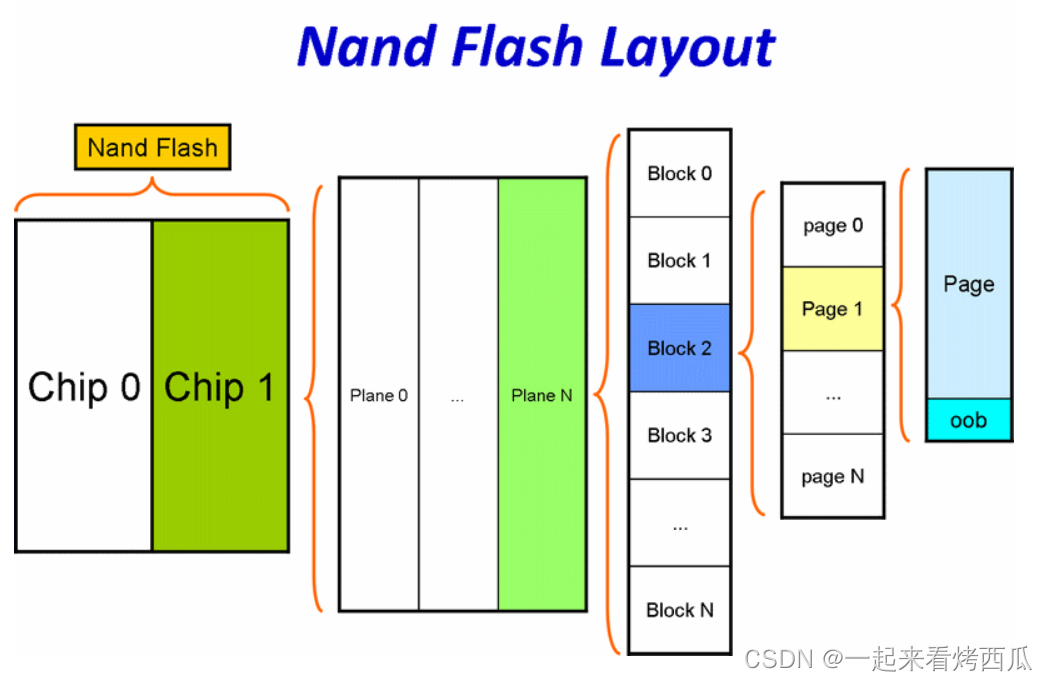
Flash Memory 即闪存,包括 NOR 与 NAND 两种。 本文将针对 NAND Flash 进行介绍,所以后面出现的闪存即 NAND Flash 。 1)NAND Flash 基本存储单元 NAND 的基本存储单元(Cell)是一种类 NMOS 的双层浮栅 MOS 管,如图所示。 闪存基本存储单元结构图 String: In NAND flash memory, a string refers to a series of memory cells connected in a sequence along a bit line. Each string usually consists of several cells, including the select transistors at both ends. 文章浏览阅读3.1k次,点赞3次,收藏12次。本文介绍了半导体存储器的分类,包括RAM、ROM和NVM,重点讲述了NAND闪存的工作原理和结构。NAND基于浮栅技术,通过改变浮栅内的电子数量来表示数据。在NAND内存阵列中,主要组成有string、page和block,其中page是逻辑上的页,block是可擦除的最小单位。每个NAND
Nowadays, Solid State Drives consume an enormous amount of NAND FlashNAND flash memories [1] causing a restless pressure on increasing the number of stored bits per mm2. Planar memory cells have been scaled for decades by improving process technology, circuit
基本单元参考 NOR FLASH 和 NAND FLASH 基本结构和特点 NAND 和 NOR Flash 完全学习笔记 Nand 基本原理 mosfet 制造工艺,场效应管制造工艺介绍-KIA MOS 管 What is NOR Flash Memory and How is it Different from NAND? 低速接口之 SPI 接口,分类,四种模式,特点 NAND vs. NOR Flash Memory – Technology Overview Why does NAND erase only at Introduction This technical note discusses the basics of NAND Flash and demonstrates its power, density, Select Gate SG transistors one and cost advantages for embedded systems. It covers data reliability and methods for overcoming common interface design challenges, focusing on the actual hardware and software components necessary to enable designers to build complete and functional subsystems. 三星的V-NAND采用了单VC垂直蚀刻工艺,最多堆叠128层 (V6);其他所有的3D NAND产品采用多层的string整合,比如英特尔的144层,3-deck,上中下各48层。
NAND Flash string with horizontal gate and vertical channel: a planar, b planar rotated by 90°, c vertical channel with cylindrical shape and d its cross section Since the very first introduction of three-dimensional (3–D) vertical-channel (VC) NAND Flash memory arrays, gate-induced drain leakage (GIDL) current has been suggested as a solution to increase the string channel potential to trigger the erase operation.
Nand Flash 来源 https://zhuanlan.zhihu.com/p/77492720 0. 引言: 最近想要从原理上了解3D Nand,搜了很多资料,发现很多资料都只侧重某一 The chip industry is pushing to quadruple the stack height of 3D NAND flash from 200 layers to 800 layers or more over the next few years, using the additional capacity will help to feed the unending need for more memory of all types. Those additional layers will add new reliability issues a number
- Nationalgericht Indien: Hyderabadi Biryani
- National Starch , National Starch & Chemical GmbH & Co. KG, Kleve
- Natrium Phosphoricum C30 1G Globuli
- Nachlassabteilung Im Amtsgericht Bernau Bei Berlin
- Naturtheater Bauerbach Grabfeld
- Nachsorge Nach Einer Hand-Operation
- Nachhaltige Fassaden: Unsere Verantwortung Ihnen Gegenüber
- Nagelform Squoval Feilen , Nagelformen und wie man sie feilt
- Nak Krefeld West Gemeinde – Gemeindevorstellung: Krefeld-Uerdingen
- Nachhaltige Filme Produzieren: Dieser Filmemacher Zeigt, Wie Das Geht
- Nachlass Gebhard Wendelin Gunz
- Nachtkulturbeauftragter – Rücktritt des Nachtkulturbeauftragen: Chance auf Neuanfang nutzen
- Nationalsozialismus ǀ Späte Ehrung — Der Freitag
- Nackt In Der Sauna, Bekannte Kommen Plötzlich Rein